
The logic cells are the digital logic components in the design. While one could create a design completely out of simple 2 input NAND logic gates, the delays in the programmable wiring, the physical size of the wiring and switching matrix relative to a logic gate, and the sheer amount of wiring needed to interconnect such small cells becomes prohibitive when considering devices capable of complex modern designs. Instead, each logic cell generally combines a few binary inputs (typically between 3 and 10) to one or two outputs according to a Boolean logic equation specified as part of the user’s device program. In most devices, the user also has an option of including or bypassing a D flip-flop attached to the outputs of the cell to make clocked sequential logic easier to implement. The logic cell may be implemented as a small memory with 2n addresses that is addressed by the n logic inputs and is pre-loaded from the user program with the values for the desired Boolean logic function. Alternatively, some devices use a small circuit of selectors set by the configuration program to combine the logic inputs in one of a number of possible ways. The memory approach provides more flexibility but at the cost of greater area and increased propagation delays compared to selector type logic. The block diagram below depicts a simplified logic cell that uses a 16x1 memory made up of digital latches. Once programmed, the memory is treated as a read-only memory addressed by the 4 bit digital input to the logic cell. By programming a ‘1’ or ‘0’ value into each of the 16 memory locations, any arbitrary Boolean logic function of the 4 inputs is produced at the memory output. This simple cell has a D flip-flop attached to the output that can be bypassed by setting the appropriate bit in the configuration program. The configurable logic blocks shown in the above section typically contain several logic cells. That collection of logic cells is usually embellished with added logic to speed up arithmetic and to add some extra features.
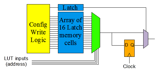 simple look-up-table (LUT) logic cell
Modern devices often have special purpose logic blocks such as Multiplier-accumulate and memory sprinkled throughout the array to make it possible to implement very complex and fast designs. These added features make signal processing far easier than it was with the early homogenous arrays containing identical cells throughout.