
Individually defining the millions of switch settings and logic cell functions would be a daunting task if done by hand. Fortunately, this task is handled by special software that converts circuit designs expressed with either schematics or a textual hardware description language into the digital code to control the configuration switches through a series of steps. The software synthesizes or elaborates the captured design into a net list (may be done by third party tools), then translates the net list into an internal representation, reconstructs that representation mapping it into logic cells, places the mapped logic cells in specific locations on the device grid, performs the routing to connect the cells according to the user’s design and finally produces the configuration bit stream used to program the device. The software monitors circuit propagation delays while it is mapping, placing and routing the design in an attempt to find a solution that meets timing, and reports the timing and utilization results. To the designer, the design capture is quite similar to design capture for other technologies. The FPGA vendors, as well as third parties also offer libraries of intellectual property (IP) designs for common circuits that can be dropped into a user design as complete functional blocks. Some of these are highly optimized for the device, and many have been thoroughly verified. These IP blocks can shorten the design cycle by leveraging off of other people’s work. Most of the FPGA software packages (these are chip vendor specific) have hooks to allow an expert user to influence the implementation, placement and routing of the design in order to obtain better performance and utilization of the device. Additionally, if the designer considers the architecture of the specific FPGA he is using while doing the design he can make the job of the implementation tools a lot easier, yielding a better finished product.
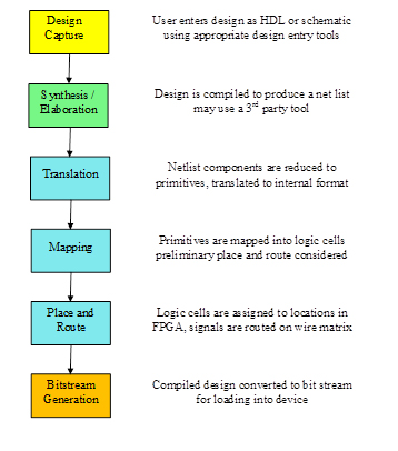 Simplified design flow for FPGA